- 您现在的位置:买卖IC网 > Sheet目录1992 > DAC8043GP (Analog Devices Inc)IC DAC 12BIT MULTIPLY CMOS 8-DIP
DAC8043
Rev. E | Page 12 of 16
APPLICATIONS INFORMATION
APPLICATION TIPS
In most applications, linearity depends upon the potential
of the IOUT and GND pins being equal to each other. In most
applications, the DAC is connected to an external op amp
with its noninverting input tied to ground (see Figure 16 and
Figure 17). The amplifier selected should have a low input bias
current and low drift over temperature. The amplifier’s input offset
voltage should be nulled to less than 200 μV (less than 10% of
1 LSB).
The noninverting input of the operational amplifier should have
a minimum resistance connection to ground; the usual bias
current compensation resistor should not be used. This resistor
can cause a variable offset voltage appearing as a varying output
error. All grounded pins should tie to a single common ground
point, avoiding ground loops. The VDD power supply should
have a low noise level with no transients greater than 17 V.
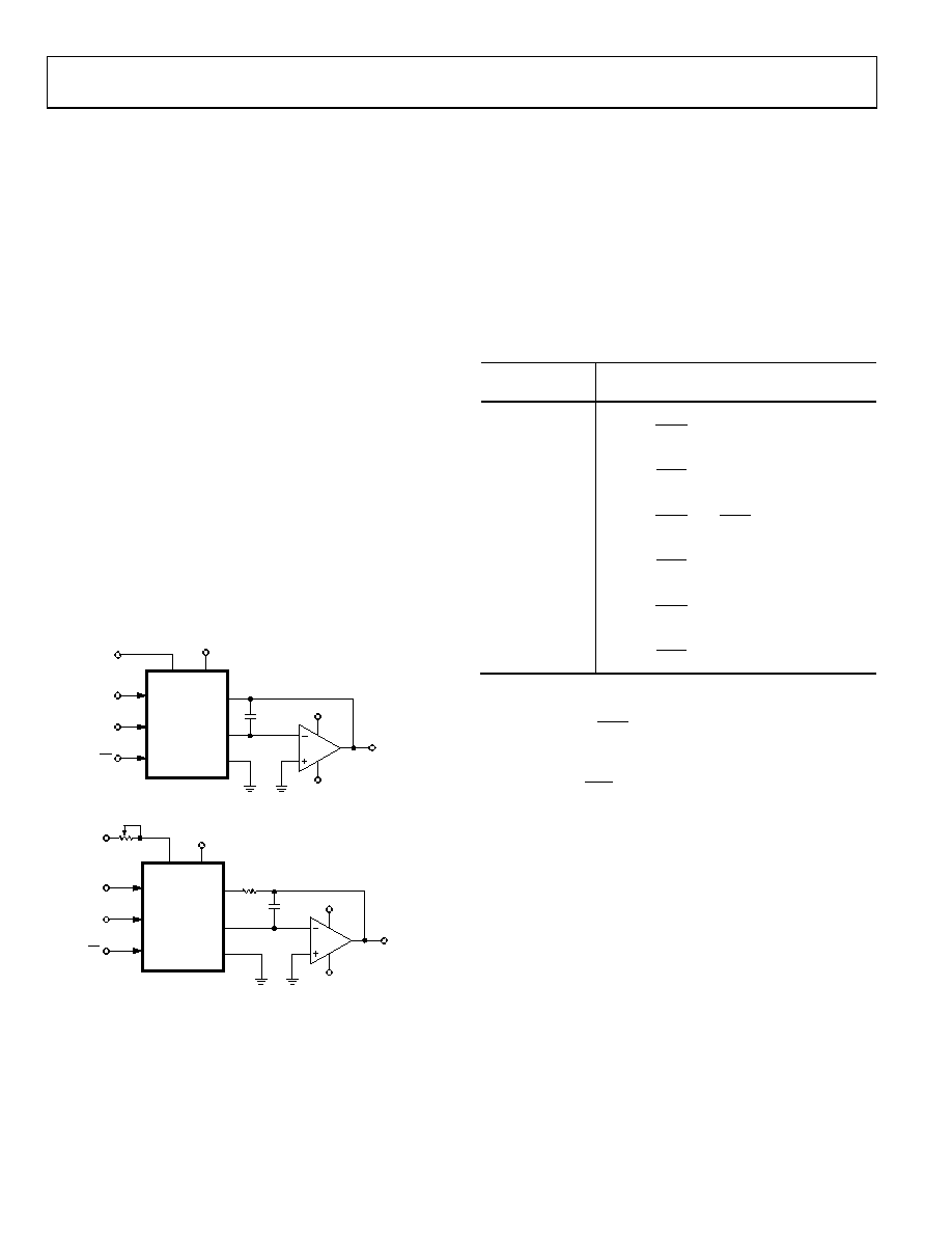
Unipolar Operation (2-Quadrant)
The circuits shown in Figure 16 and Figure 17 may be used with
an ac or dc reference voltage. The output of the circuit ranges
between 0 V and approximately VREF (4095/4096), depending
upon the digital input code. The relationship between the
digital input and the analog output is shown in Table 6. The
limiting parameters for the VREF range are the maximum input
voltage range of the op amp or ±25 V, whichever is lowest.
00271-
016
OP77
DAC8043
3
2
6
4
7
+15V
5V
15pF
VOUT
RFB
VDD
VREF
IOUT
GND
SERIAL
DATA
INPUT
CLK
VREF
10V
–15V
LD
Figure 16. Unipolar Operation with High Accuracy Op Amp (2-Quadrant)
00271-
017
OP42
DAC8043
2
3
6
4
7
+15V
5V
15pF
VOUT
RFB
VDD
VREF
IOUT
GND
SERIAL
DATA
INPUT
CLK
VREF
10V
R2
50
R1
100
–15V
LD
Figure 17. Unipolar Operation with Fast Op Amp and Gain Error Trimming
(2-Quadrant)
The DAC register must first be loaded with all 1s. R1 may then
be adjusted until VOUT = VREF (4095/4096). In the case of an
adjustable VREF, R1 and R2 may be omitted, with VREF adjusted
to yield the desired full-scale output.
In most applications, the DAC8043’s negligible zero-scale error
and very low gain error permit the elimination of the trimming
components (R1 and the external R2) without adversely affecting
on circuit performance.
Table 6. Unipolar Code Table1, 2
Digital Input
Nominal Analog Output
MSB
LSB
(V
OUT as Shown in Figure 16 and Figure 17)
1111 1111 1111
4096
4095
REF
V
1000 0000 0001
4096
2049
REF
V
1000 0000 0000
2
4096
2048
REF
V
=
0111 1111 1111
4096
2047
REF
V
0000 0000 0001
4096
1
REF
V
0000 0000 0000
0
4096
0
=
REF
V
1 Nominal full scale for Figure 16 and Figure 17 circuits is given by
=
4096
4095
REF
V
FS
2 Nominal LSB magnitude for Figure 16 and Figure 17 circuits is given by
( )n
REF
V
LSB
=
2
or
4096
1
发布紧急采购,3分钟左右您将得到回复。
相关PDF资料
DAC8221GP
IC DAC 12BIT DUAL W/BUFF 24-DIP
DAC8222GPZ
IC DAC 12BIT DUAL W/BUFF 24DIP
DAC8229FSZ-REEL
IC DAC 8BIT DUAL V-OUT 20SOIC
DAC8248FS
IC DAC 12BIT DUAL W/BUFF 24-SOIC
DAC8408GP
IC DAC 8BIT QUAD W/MEMORY 28-DIP
DAC8413EP
IC DAC 12BIT QUAD V-OUT 28-DIP
DAC8420FQ
IC DAC 12BIT QUAD SRL LP 16-CDIP
DAC8426EPZ
IC DAC 8BIT QUAD 10VREF 20PDIP
相关代理商/技术参数
DAC8043GPZ
功能描述:IC DAC 12BIT MULTIPLY CMOS 8-DIP RoHS:是 类别:集成电路 (IC) >> 数据采集 - 数模转换器 系列:- 产品培训模块:Data Converter Fundamentals
DAC Architectures 标准包装:750 系列:- 设置时间:7µs 位数:16 数据接口:并联 转换器数目:1 电压电源:双 ± 功率耗散(最大):100mW 工作温度:0°C ~ 70°C 安装类型:表面贴装 封装/外壳:28-LCC(J 形引线) 供应商设备封装:28-PLCC(11.51x11.51) 包装:带卷 (TR) 输出数目和类型:1 电压,单极;1 电压,双极 采样率(每秒):143k
DAC8043HP
制造商:Analog Devices 功能描述: 制造商:PMI/AD 功能描述:
DAC8043U
功能描述:数模转换器- DAC 12bit Multiply D/A RoHS:否 制造商:Texas Instruments 转换器数量:1 DAC 输出端数量:1 转换速率:2 MSPs 分辨率:16 bit 接口类型:QSPI, SPI, Serial (3-Wire, Microwire) 稳定时间:1 us 最大工作温度:+ 85 C 安装风格:SMD/SMT 封装 / 箱体:SOIC-14 封装:Tube
DAC8043U
制造商:Texas Instruments 功能描述:D/A Converter (D-A) IC 制造商:Texas Instruments 功能描述:IC, DAC, 12BIT, 284KSPS, SOIC-8
DAC8043U/2K5
功能描述:数模转换器- DAC 12bit Multiply D/A RoHS:否 制造商:Texas Instruments 转换器数量:1 DAC 输出端数量:1 转换速率:2 MSPs 分辨率:16 bit 接口类型:QSPI, SPI, Serial (3-Wire, Microwire) 稳定时间:1 us 最大工作温度:+ 85 C 安装风格:SMD/SMT 封装 / 箱体:SOIC-14 封装:Tube
DAC8043U/2K5G4
功能描述:数模转换器- DAC 12bit Multiply D/A RoHS:否 制造商:Texas Instruments 转换器数量:1 DAC 输出端数量:1 转换速率:2 MSPs 分辨率:16 bit 接口类型:QSPI, SPI, Serial (3-Wire, Microwire) 稳定时间:1 us 最大工作温度:+ 85 C 安装风格:SMD/SMT 封装 / 箱体:SOIC-14 封装:Tube
DAC8043U2K5
制造商:TI 制造商全称:Texas Instruments 功能描述:CMOS 12-Bit Serial Input Multiplying DIGITAL-TO-ANALOG CONVERTER
DAC8043U2K5G4
制造商:TI 制造商全称:Texas Instruments 功能描述:CMOS 12-Bit Serial Input Multiplying DIGITAL-TO-ANALOG CONVERTER